- 您现在的位置:买卖IC网 > Sheet目录492 > NTMSD3P102R2G (ON Semiconductor)MOSFET P-CH 20V 2.34A 8-SOIC
�� �
�
�NTMSD3P102R2�
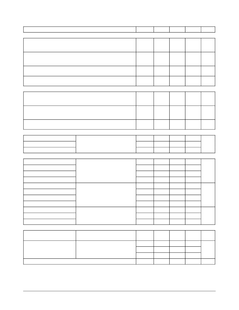
�MOSFET� ELECTRICAL� CHARACTERISTICS� (T� J� =� 25� °� C� unless� otherwise� noted)� (Note� 9)�
�Characteristic�
�Symbol�
�Min�
�Typ�
�Max�
�Unit�
�OFF� CHARACTERISTICS�
�Drain-to-Source� Breakdown� Voltage�
�(V� GS� =� 0� Vdc,� I� D� =� -250� m� Adc)�
�Temperature� Coefficient� (Positive)�
�Zero� Gate� Voltage� Drain� Current�
�(V� DS� =� -20� Vdc,� V� GS� =� 0� Vdc,� T� J� =� 25� °� C)�
�(V� DS� =� -20� Vdc,� V� GS� =� 0� Vdc,� T� J� =� 125� °� C)�
�V� (BR)DSS�
�I� DSS�
�-20�
�-�
�-�
�-�
�-�
�-30�
�-�
�-�
�-�
�-�
�-1.0�
�-25�
�Vdc�
�mV/� °� C�
�m� Adc�
�Gate-Body� Leakage� Current�
�I� GSS�
�nAdc�
�(V� GS� =� -20� Vdc,� V� DS� =� 0� Vdc)�
�Gate-Body� Leakage� Current�
�(V� GS� =� +20� Vdc,� V� DS� =� 0� Vdc)�
�I� GSS�
�-�
�-�
�-�
�-�
�-100�
�100�
�nAdc�
�ON� CHARACTERISTICS�
�Gate� Threshold� Voltage�
�(V� DS� =� V� GS� ,� I� D� =� -250� m� Adc)�
�Temperature� Coefficient� (Negative)�
�V� GS(th)�
�-1.0�
�-�
�-1.7�
�3.6�
�-2.5�
�-�
�Vdc�
�Static� Drain-to-Source� On-State� Resistance�
�R� DS(on)�
�W�
�(V� GS� =� -10� Vdc,� I� D� =� -3.05� Adc)�
�(V� GS� =� -4.5� Vdc,� I� D� =� -1.5� Adc)�
�Forward� Transconductance�
�(V� DS� =� -15� Vdc,� I� D� =� -3.05� Adc)�
�g� FS�
�-�
�-�
�-�
�0.063�
�0.090�
�5.0�
�0.085�
�0.125�
�-�
�Mhos�
�DYNAMIC� CHARACTERISTICS�
�Input� Capacitance�
�C� iss�
�-�
�518�
�750�
�pF�
�Output� Capacitance�
�Reverse� Transfer� Capacitance�
�(V� DS� =� -16� Vdc,� V� GS� =� 0� Vdc,�
�f� =� 1.0� MHz)�
�C� oss�
�C� rss�
�-�
�-�
�190�
�70�
�350�
�135�
�SWITCHING� CHARACTERISTICS� (Notes� 10� &� 11)�
�Turn-On� Delay� Time�
�t� d(on)�
�-�
�12�
�22�
�ns�
�Rise� Time�
�Turn-Off� Delay� Time�
�Fall� Time�
�(V� DD� =� -20� Vdc,� I� D� =� -3.05� Adc,�
�V� GS� =� -10� Vdc,�
�R� G� =� 6.0� W� )�
�t� r�
�t� d(off)�
�t� f�
�-�
�-�
�-�
�16�
�45�
�45�
�30�
�80�
�80�
�Turn-On� Delay� Time�
�t� d(on)�
�-�
�16�
�-�
�ns�
�Rise� Time�
�Turn-Off� Delay� Time�
�Fall� Time�
�(V� DD� =� -20� Vdc,� I� D� =� -1.5� Adc,�
�V� GS� =� -4.5� Vdc,�
�R� G� =� 6.0� W� )�
�t� r�
�t� d(off)�
�t� f�
�-�
�-�
�-�
�42�
�32�
�35�
�-�
�-�
�-�
�Total� Gate� Charge�
�Gate-Source� Charge�
�Gate-Drain� Charge�
�(V� DS� =� -20� Vdc,�
�V� GS� =� -10� Vdc,�
�I� D� =� -3.05� Adc)�
�Q� tot�
�Q� gs�
�Q� gd�
�-�
�-�
�-�
�16�
�2.0�
�4.5�
�25�
�-�
�-�
�nC�
�BODY-DRAIN� DIODE� RATINGS� (Note� 10)�
�Diode� Forward� On-Voltage�
�Reverse� Recovery� Time�
�(I� S� =� -3.05� Adc,� V� GS� =� 0� Vdc)�
�(I� S� =� -3.05� Adc,� V� GS� =� 0� Vdc,� T� J� =� 125� °� C)�
�(I� S� =� -3.05� Adc,� V� GS� =� 0� Vdc,�
�dI� S� /dt� =� 100� A/� m� s)�
�V� SD�
�t� rr�
�t� a�
�-�
�-�
�-�
�-�
�-0.96�
�-0.78�
�34�
�18�
�-1.25�
�-�
�-�
�-�
�Vdc�
�ns�
�t� b�
�-�
�16�
�-�
�Reverse� Recovery� Stored� Charge�
�Q� RR�
�-�
�0.03�
�-�
�m� C�
�9.� Handling� precautions� to� protect� against� electrostatic� discharge� are� mandatory.�
�10.� Indicates� Pulse� Test:� Pulse� Width� =� 300� m� s� max,� Duty� Cycle� =� 2%.�
�11.� Switching� characteristics� are� independent� of� operating� junction� temperature.�
�http://onsemi.com�
�3�
�发布紧急采购,3分钟左右您将得到回复。
相关PDF资料
NTMSD3P303R2G
MOSFET P-CH 30V 2.34A 8-SOIC
NTMSD6N303R2G
MOSFET N-CH 30V 6A 8-SOIC
NTNUS3171PZT5G
MOSFET P-CH 20V 200MA SOT-1123
NTP125N02RG
MOSFET N-CH 24V 15.9A TO220AB
NTP18N06G
MOSFET N-CH 60V 15A TO220AB
NTP18N06LG
MOSFET N-CH 60V 15A TO220AB
NTP2955
MOSFET P-CH 60V 2.4A TO220AB
NTP30N06LG
MOSFET N-CH 60V 30A TO220AB
相关代理商/技术参数
NTMSD3P102R2SG
功能描述:MOSFET FETKY 20V .085R TR RoHS:否 制造商:STMicroelectronics 晶体管极性:N-Channel 汲极/源极击穿电压:650 V 闸/源击穿电压:25 V 漏极连续电流:130 A 电阻汲极/源极 RDS(导通):0.014 Ohms 配置:Single 最大工作温度: 安装风格:Through Hole 封装 / 箱体:Max247 封装:Tube
NTMSD3P303
制造商:ONSEMI 制造商全称:ON Semiconductor 功能描述:Typical Uses for FETKY Devices
NTMSD3P303R2
功能描述:MOSFET -30V -3.05A RoHS:否 制造商:STMicroelectronics 晶体管极性:N-Channel 汲极/源极击穿电压:650 V 闸/源击穿电压:25 V 漏极连续电流:130 A 电阻汲极/源极 RDS(导通):0.014 Ohms 配置:Single 最大工作温度: 安装风格:Through Hole 封装 / 箱体:Max247 封装:Tube
NTMSD3P303R2/D
制造商:未知厂家 制造商全称:未知厂家 功能描述:FETKY?
NTMSD3P303R2_06
制造商:ONSEMI 制造商全称:ON Semiconductor 功能描述:P-Channel Enhancement-Mode Power MOSFET and Schottky Diode Dual SO-8 Package
NTMSD3P303R2G
功能描述:MOSFET -30V -3.05A P-Channel RoHS:否 制造商:STMicroelectronics 晶体管极性:N-Channel 汲极/源极击穿电压:650 V 闸/源击穿电压:25 V 漏极连续电流:130 A 电阻汲极/源极 RDS(导通):0.014 Ohms 配置:Single 最大工作温度: 安装风格:Through Hole 封装 / 箱体:Max247 封装:Tube
NTMSD6N303
制造商:ONSEMI 制造商全称:ON Semiconductor 功能描述:Typical Uses for FETKY Devices
NTMSD6N303R2
功能描述:MOSFET 30V 6A N-Channel RoHS:否 制造商:STMicroelectronics 晶体管极性:N-Channel 汲极/源极击穿电压:650 V 闸/源击穿电压:25 V 漏极连续电流:130 A 电阻汲极/源极 RDS(导通):0.014 Ohms 配置:Single 最大工作温度: 安装风格:Through Hole 封装 / 箱体:Max247 封装:Tube